01 / HARVEST
Concentrating light in thin films
Metal-nanoparticle scattering, grating-coupled surface plasmons, and waveguide modes increase the optical path length and absorption within thin active layers.
We integrate metal nanostructures, periodic gratings, and engineered optical interfaces into the thin absorbing layers of organic solar cells—trapping more light and strengthening absorption and charge generation within a limited film thickness.
Organic solar cells are flexible, lightweight, and compatible with low-temperature processing. Yet exciton diffusion and charge-transport constraints limit absorber thickness, making it essential to increase optical harvesting without compromising charge extraction.
Metal-nanoparticle scattering, grating-coupled surface plasmons, and waveguide modes increase the optical path length and absorption within thin active layers.
Particle shape, size, placement, and grating period are combined to align localized and propagating optical modes with the absorber spectrum.
Nanomaterial loading and insertion layers are optimized to benefit from near fields and scattering while limiting recombination and transport resistance.
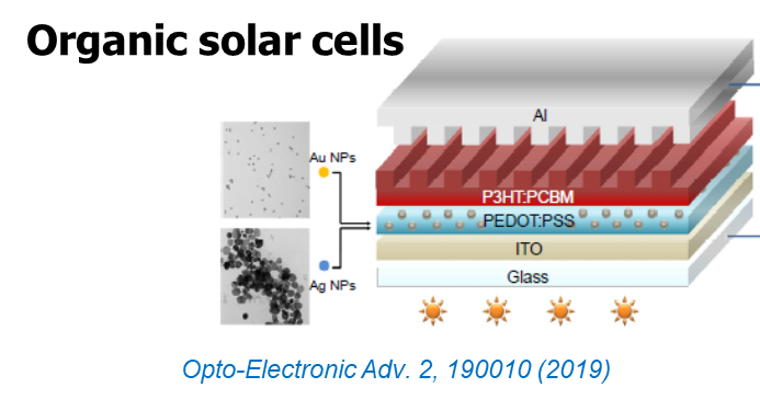
From light trapping in wet-type dye-sensitized and P3HT:PCBM organic thin-film solar cells to non-fullerene PM6:Y6 and PM6:Y7 systems, we have evolved plasmonic structures and their placement in step with each generation of photovoltaic materials.
Metal nanostructures are treated not as isolated additives but as optical elements within the complete multilayer device—including the active layer, transport layers, metal electrodes, and periodic structures.
Gold nanospheres, nanorods, nanourchins, nanostars, and silver nanoprisms tune resonance wavelength, scattering, and tip-enhanced fields.
Blu-ray-derived periodic patterns and metallic gratings excite propagating plasmons and waveguide modes that redirect light into the active layer.
Mixed particle morphologies and nanoparticle–grating combinations create broadband scattering, near-field enhancement, and coupled resonances.
Designs are extended to PM6:Y6 and PM6:Y7 absorbers and AZO electron-transport layers, matching particle morphology and loading to optical absorption and charge transport.
The work began by introducing plasmonic structures into wet-type dye-sensitized and organic thin-film solar cells, expanded to hybrid optical designs combining metal nanoparticles, gratings, quantum dots, and anisotropic particles, and now targets high-performance non-fullerene devices.
Blu-ray-derived gratings coupled propagating surface-plasmon fields into Au/TiO₂/dye/electrolyte interfaces in wet-type dye-sensitized solar cells and into Ag/P3HT:PCBM interfaces in organic thin-film cells. These studies established the light-concentration concept that underpins our current work.
TiO₂ thin films and metal-loaded TiO₂/dye composite films on gold gratings were used to investigate photocurrent enhancement by simultaneously exploiting localized nanoparticle plasmons and grating-coupled propagating plasmons. This marked the transition from single resonances to coupled plasmonic design.
Studies demonstrated localized-plasmon enhancement from gold nanourchins, grating-coupled plasmons and waveguide modes in inverted cells, and light trapping using Blu-ray-derived gratings.
Silver nanodisks on gratings, gold quantum dots with gold nanoparticles, one- and two-dimensional gratings, and mixed silver nanoprisms enabled several optical mechanisms to operate together.
Our accumulated work on gold nanostructures and quantum dots was consolidated in a review, while gold and silver nanoparticles were introduced into PM6:Y7 and PM6:Y6 devices to adapt LSPR design to next-generation absorbers.
Gold nanostars and gold nanoparticles were co-embedded in the AZO electron-transport layer, combining tip-enhanced fields, broadband coupling, and scattering. The PM6:Y6 cell reached a maximum power-conversion efficiency of 12.36%, while experiments and FDTD analysis showed why particle loading must be carefully optimized.
Our perovskite-solar-cell work is at an early stage. Building on expertise in thin-film formation, optical interfaces, nanostructures, and charge transport developed through organic photovoltaics, we are exploring device structures that combine efficient light use with improved stability.
PHYSICAL CHEMISTRY CHEMICAL PHYSICS
JAPANESE JOURNAL OF APPLIED PHYSICS
NANOSCALE ADVANCES · REVIEW
JOURNAL OF SCIENCE: ADVANCED MATERIALS AND DEVICES
ROYAL SOCIETY OPEN SCIENCE
NANOSCALE ADVANCES
OPTO-ELECTRONIC ADVANCES
NANOSCALE ADVANCES
PARTICLE & PARTICLE SYSTEMS CHARACTERIZATION
NANOSCALE
PHYSICAL CHEMISTRY CHEMICAL PHYSICS
PHYSICAL CHEMISTRY CHEMICAL PHYSICS
PHYSICAL CHEMISTRY CHEMICAL PHYSICS
SURFACE AND INTERFACE ANALYSIS
ACS APPLIED MATERIALS & INTERFACES
JOURNAL OF MATERIALS CHEMISTRY
We collaborate on projects combining organic and perovskite photovoltaics, metallic nanomaterials, periodic structures, thin-film processing, and optical and electrical characterization.
✉ Discuss a collaboration ↗